Showing posts with label 555 timer circuits. Show all posts
Monday, October 12, 2009

555 Timer IC Working Principle

555 timer Block Diagram

555 timer Block Diagram

Block diagram for the 555 timer is given in figure. As shown in the block diagram, a 555 timer consists of two comparators (simply op-amps), an R-S flip-flop, two transistors and a resistive network

  • Resistive network consists of three equal resistors and acts as a voltage divider.
  • Comparator 1 compares threshold voltage with a reference voltage + 2/3 VCC volts.
  • Comparator 2 compares the trigger voltage with a reference voltage + 1/3 VCC volts.

Output of both the comparators is supplied to the flip-flop. Flip-flop assumes its state according to the output of the two compa­rators.

One of the two transistors is a discharge transis­tor of which collector is connected to pin 7. This tran­sistor saturates or cuts-off according to the output state of the flip-flop. The saturated transis­tor provides a discharge path to a capacitor con­nected externally. Base of another transistor is connected to a reset terminal. A pulse applied to this terminal resets the whole timer irrespective of any input.
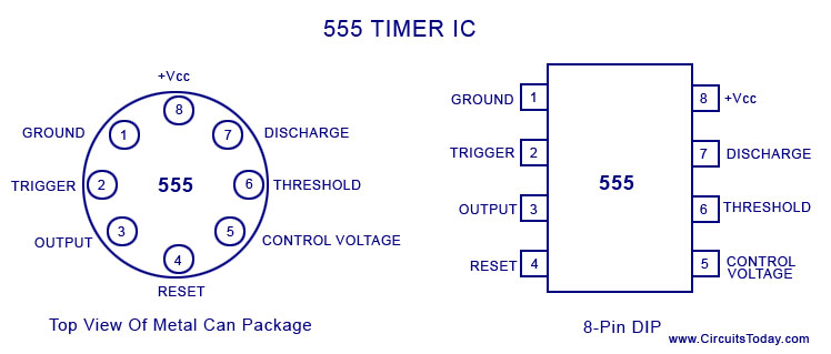
555 Timer IC Packages

555 Timer IC Packages

The 555 Timer IC is available as an 8-pin metal can, an 8-pin mini DIP (dual-in-package) or a 14-pin DIP.

This IC consists of 23 transistors, 2 diodes and 16 resistors. The explanation of terminals coming out of the 555 timer IC is as follows. The pin number used in the following discussion refers to the 8-pin DIP and 8-pin metal can packages.

555 timer ic 14 pin configuration

555 timer ic 14 pin configuration

Pin 1: Grounded Terminal. All the voltages are meas­ured with respect to this terminal.

Pin 2: Trigger Terminal. This pin is an inverting input to a comparator that is responsible for transition of flip-flop from set to reset. The output of the timer depends on the amplitude of the external trigger pulse applied to this pin.

Pin 3: Output Terminal. Output of the timer is avail­able at this pin. There are two ways in which a load can be connected to the output terminal either between pin 3 and ground pin (pin 1) or between pin 3 and supply pin (pin 8). The load connected between pin 3 and ground

supply pin is called the normally on load and that connected between pin 3 and ground pin is called the normally off load.

Pin 4: Reset Terminal. To disable or reset the timer a negative pulse is applied to this pin due to which it is referred to as reset terminal. When this pin is not to be used for reset purpose, it should be connected to + VCC to avoid any possibility of false triggering.

Pin 5: Control Voltage Terminal. The function of this terminal is to control the threshold and trigger levels. Thus either the external voltage or a pot connected to this pin determines the pulse width of the output waveform. The external voltage applied to this pin can also be used to modulate the output waveform. When this pin is not used, it should be connected to ground through a 0.01 micro Farad to avoid any noise problem.

Pin 6: Threshold Terminal. This is the non-inverting input terminal of comparator 1, which compares the voltage applied to the terminal with a reference voltage of 2/3 VCC. The amplitude of voltage applied to this terminal is responsible for the set state of flip-flop.

Pin 7 : Discharge Terminal. This pin is connected internally to the collector of transistor and mostly a capacitor is connected between this terminal and ground. It is called discharge terminal because when transistor saturates, capacitor discharges through the transistor. When the transistor is cut-off, the capacitor charges at a rate determined by the external resistor and capacitor.

Pin 8: Supply Terminal. A supply voltage of + 5 V to + 18 V is applied to this terminal with respect to ground (pin 1).

WORKING PRINCPLE:

Comparator 1 has a threshold input (pin 6) and a control input (pin 5). In most applications, the control input is not used, so that the control voltage equals +2/3 VCC. Output of this comparator is applied to set (S) input of the flip-flop. Whenever the threshold voltage exceeds the control voltage, comparator 1 will set the flip-flop and its output is high. A high output from the flip-flop saturates the discharge transistor and discharge the capacitor connected externally to pin 7. The complementary signal out of the flip-flop goes to pin 3, the output. The output available at pin 3 is low. These conditions will prevail until comparator 2 triggers the flip-flop. Even if the voltage at the threshold input falls below 2/3 VCC, that is comparator 1 cannot cause the flip-flop to change again. It means that the comparator 1 can only force the flip-flop’s output high.

To change the output of flip-flop to low, the voltage at the trigger input must fall below + 1/3 Vcc. When this occurs, comparator 2 triggers the flip-flop, forcing its output low. The low output from the flip-flop turns the discharge transistor off and forces the power amplifier to output a high. These conditions will continue independent of the voltage on the trigger input. Comparator 2 can only cause the flip-flop to output low.

From the above discussion it is concluded that for the having low output from the timer 555, the voltage on the threshold input must exceed the control voltage or + 2/3 VCC. They also turn the discharge transistor on. To force the output from the timer high, the voltage on the trigger input must drop below +1/3 VCC. This also turns the discharge transistor off.

A voltage may be applied to the control input to change the levels at which the switching occurs. When not in use, a 0.01 nano Farad capacitor should be connected between pin 5 and ground to prevent noise coupled onto this pin from causing false triggering.

Connecting the reset (pin 4) to a logic low will place a high on the output of flip-flop. The discharge transistor will go on and the power amplifier will output a low. This condition will continue until reset is taken high. This allows synchronization or resetting of the circuit’s operation. When not in use, reset should be tied to +VCC.

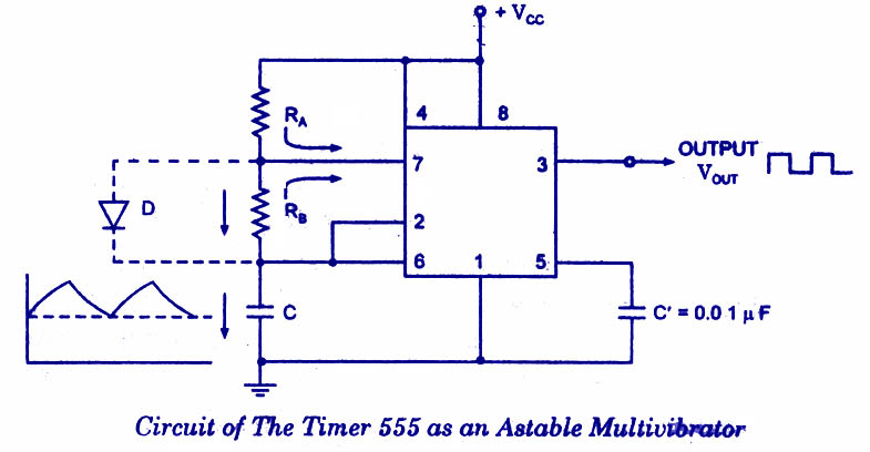
An astable multivibrator, often called a free-running multivibrator, is a rectan­gular-wave generating cir­cuit. Unlike the monostable multivibrator, this circuit does not require any ex­ternal trigger to change the state of the output, hence the name free-running. Before going to make the circuit, make sure your 555 IC is working. For that go through the article: How to test a 555 IC for working An astable multivibrator can be produced by adding resistors and a capacitor to the basic timer IC, as illustrated in figure. The timing during which the output is either high or low is determined by the externally connected two resistors and a capacitor. The details of the astable multivibrator circuit are given below.

555-Astable-Multivibrator

Take a look @ 555 Ic Pin configuration and 555 block diagram before reading further.

Pin 1 is grounded; pins 4 and 8 are shorted and then tied to supply +Vcc, output (VOUT is taken form pin 3; pin 2 and 6 are shorted and the connected to ground through capacitor C, pin 7 is connected to supply + VCC through a resistor RA; and between pin 6 and 7 a resistor RB is connected. At pin 5 either a bypass capacitor of 0.01 F is connected or modulation input is applied.

Astable Multivibrator Operation

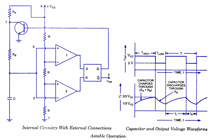
For explaining the operation of the timer 555 as an astable multivibrator, necessary internal circuitry with external connections are shown in figure.

Astable-Multivibrator-Operation

In figure, when Q is low or output VOUT is high, the discharging transistor is cut-­off and the capacitor C begins charging toward VCC through resistances RA and RB. Because of this, the charging time constant is (RA + RB) C. Eventually, the threshold voltage exceeds +2/3 VCC, the comparator 1 has a high output and triggers the flip-flop so that its Q is high and the timer output is low. With Q high, the discharge transistor saturates and pin 7 grounds so that the capacitor C discharges through resistance RB with a discharging time constant RB C. With the discharging of capacitor, trigger voltage at inverting input of comparator 2 decreases. When it drops below 1/3VCC, the output of comparator 2 goes high and this reset the flip-flop so that Q is low and the timer output is high. This proves the auto-transition in output from low to high and then to low as, illustrated in fig ures. Thus the cycle repeats.

Astable Multivibrator using 555 IC -Design method

The time during which the capacitor C charges from 1/3 VCC to 2/3 VCC is equal to the time the output is high and is given as tc or THIGH = 0.693 (RA + RB) C, which is proved below.

Voltage across the capacitor at any instant during charging period is given as,vc=VCC(1-et/RC)

The time taken by the capacitor to charge from 0 to +1/3 VCC

1/3 VCC = VCC (1-et/RC)

The time taken by the capacitor to charge from 0 to +2/3 VCC

or t2 = RC loge 3 = 1.0986 RC

So the time taken by the capacitor to charge from +1/3 VCC to +2/3 VCC

tc = (t2 – t1) = (10986 – 0.405) RC = 0.693 RC

Substituting R = (RA + RB) in above equation we have

THIGH = tc = 0.693 (RA + RB) C

where RA and RB are in ohms and C is in farads.

The time during which the capacitor discharges from +2/3 VCC to +1/3 VCC is equal to

the time the output is low and is given as

td or TL0W = 0.693 RB C where RB is in ohms and C is in farads The above equation is worked out as follows: Voltage across the capacitor at any instant during discharging period is given as

vc = 2/3 VCC e- td/ RBC

Substituting vc = 1/3 VCC and t = td in above equation we have

+1/3 VCC = +2/3 VCC e- td/ RBC

Or td = 0.693 RBC

Overall period of oscillations, T = THIGH + TLOW = 0.693 (RA+ 2RB) C , The frequency of oscillations being the reciprocal of the overall period of oscillations T is given as

f = 1/T = 1.44/ (RA+ 2RB)C

Equation indicates that the frequency of oscillation / is independent of the collector supply voltage +VCC.

Often the term duty cycle is used in conjunction with the astable multivibrator.

The duty cycle, the ratio of the time tc during which the output is high to the total time period T is given as

% duty cycle, D = tc / T * 100 = (RA + RB) / (RA + 2RB) * 100

From the above equation it is obvious that square wave (50 % duty cycle) output can not be obtained unless RA is made zero. However, there is a danger in shorting resistance RA to zero. With RA = 0 ohm, terminal 7 is directly connected to + VCC. During the discharging of capacitor through RB and transistor, an extra current will be supplied to the transistor from VCC through a short between pin 7 and +VCC. It may damage the transistor and hence the timer.

However, a symmetrical square wave can be obtained if a diode is connected across resistor RB, as illustrated in dotted lines in figure. The capacitor C charges through RA and diode D to approximately + 2/3VCC and discharges through resistor RB and terminal 7 (transistor) until the capacitor voltage drops to 1/3 VCC. Then the cycle is repeated. To obtain a square wave output, RA must be a combination of a fixed resistor R and a pot, so that the pot can be adjusted to give the exact square wave.

Although the timer 555 has been used in a wide variety of often unique applications it is very hard on its power supply lines, requiring quite a bit of current, and injecting many noise transients. This noise will often be coupled into adjacent ICs falsely triggering them. The 7555 is a CMOS version of the 555. Its quiescent current requirements are considerably lower than that of 555, and the 7555 does not contaminate the power supply lines. It is pin compatible with the 555. So this CMOS version of the 555 should be the first choice when a 555 timer IC is to be used.

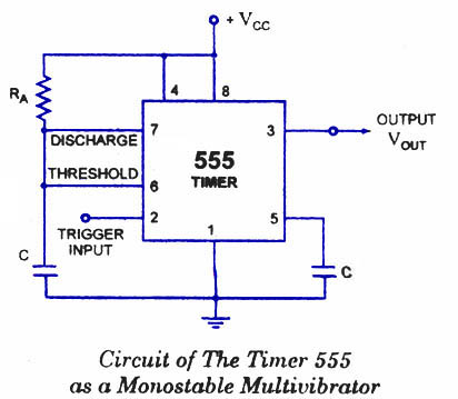
A monostable multivibrator (MMV) often called a one-shot multivibrator, is a pulse generator circuit in which the duration of the pulse is determined by the R-C network,connected externally to the 555 timer. In such a vibrator, one state of output is stable while the other is quasi-stable (unstable). For auto-triggering of output from quasi-stable state to stable state energy is stored by an externally connected capaci­tor C to a reference level. The time taken in storage determines the pulse width. The transition of output from stable state to quasi-stable state is accom­plished by external triggering. The schematic of a 555 timer in monostable mode of operation is shown in figure.

555-timer-monostable-multivibrator

555-timer-monostable-multivibrator

Monostable Multivibrator Circuit details

Pin 1 is grounded. Trigger input is applied to pin 2. In quiescent condition of output this input is kept at + VCC. To obtain transition of output from stable state to quasi-stable state, a negative-going pulse of narrow width (a width smaller than expected pulse width of output waveform) and amplitude of greater than + 2/3 VCC is applied to pin 2. Output is taken from pin 3. Pin 4 is usually connected to + VCC to avoid accidental reset. Pin 5 is grounded through a 0.01 u F capacitor to avoid noise problem. Pin 6 (threshold) is shorted to pin 7. A resistor RA is connected between pins 6 and 8. At pins 7 a discharge capacitor is connected while pin 8 is connected to supply VCC.

555 IC Monostable Multivibrator Operation.

555 monostable-multivibrator-operation

555 monostable-multivibrator-operation

For explain­ing the operation of timer 555 as a monostable multivibrator, necessary in­ternal circuitry with external connections are shown in figure.

The operation of the circuit is ex­plained below:

Initially, when the output at pin 3 is low i.e. the circuit is in a stable state, the transistor is on and capacitor- C is shorted to ground. When a negative pulse is applied to pin 2, the trigger input falls below +1/3 VCC, the output of comparator goes high which resets the flip-flop and consequently the transistor turns off and the output at pin 3 goes high. This is the transition of the output from stable to quasi-stable state, as shown in figure. As the discharge transistor is cut­off, the capacitor C begins charging toward +VCC through resistance RA with a time constant equal to RAC. When the increasing capacitor voltage becomes slightly greater than +2/3 VCC, the output of comparator 1 goes high, which sets the flip-flop. The transistor goes to saturation, thereby discharging the capacitor C and the output of the timer goes low, as illustrated in figure.

Thus the output returns back to stable state from quasi-stable state.

The output of the Monostable Multivibrator remains low until a trigger pulse is again applied. Then the cycle repeats. Trigger input, output voltage and capacitor voltage waveforms are shown in figure.

Monostable Multivibrator Design Using 555 timer IC

The capacitor C has to charge through resistance RA. The larger the time constant RAC, the longer it takes for the capacitor voltage to reach +2/3VCC.

In other words, the RC time constant controls the width of the output pulse. The time during which the timer output remains high is given as

tp = 1.0986 RAC
where RA is in ohms and C is in farads. The above relation is derived as below. Voltage across the capacitor at any instant during charging period is given as

vc = VCC (1- e-t/RAC)

Substituting vc = 2/3 VCC in above equation we get the time taken by the capacitor to charge from 0 to +2/3VCC.

So +2/3VCC. = VCC. (1 – e-t/RAC) or t – RAC loge 3 = 1.0986 RAC

So pulse width, tP = 1.0986 RAC s 1.1 RAC

The pulse width of the circuit may range from micro-seconds to many seconds. This circuit is widely used in industry for many different timing applications.

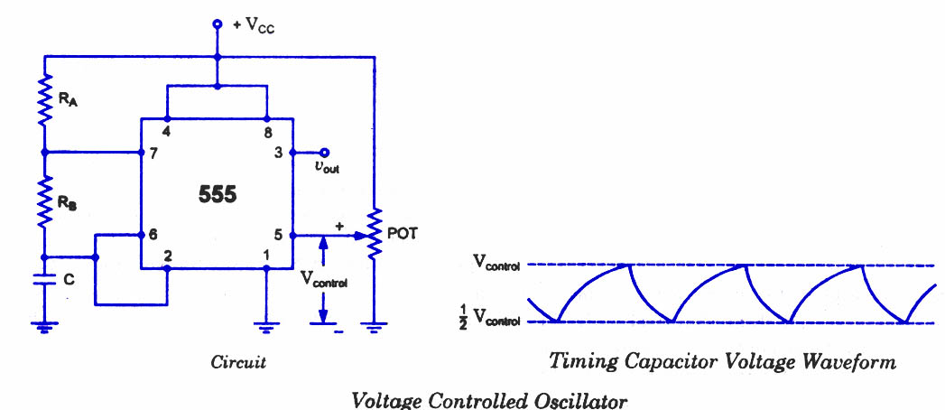
A voltage-controlled oscillator (VCO) using the timer 555 is shown in figure.

555-timer-voltage-controlled-oscillator

555-timer-voltage-controlled-oscillator

The circuit is sometimes called a voltage-to-frequency converter because the output frequency can be changed by changing the input voltage.

As discussed in previous blog posts, pin 5 terminal is voltage control terminal and its function is to control the threshold and trigger levels. Normally, the control voltage is ++2/3VCC because of the internal voltage divider. However, an external voltage can be applied to this terminal directly or through a pot, as illustrated in figure, and by adjusting the pot, control voltage can be varied. Voltage across the timing capacitor is depicted in figure, which varies between +Vcontrol and ½ Vcontrol. If control voltage is increased, the capacitor takes a longer to charge and discharge; the frequency, therefore, decreases. Thus the fre­quency can be changed by changing the control volt­age. Incidentally, the control voltage may be made available through a pot, or it may be output of a transistor circuit, op-amp, or some other device.

Ramp Generator Circuit-using 555 Timer IC

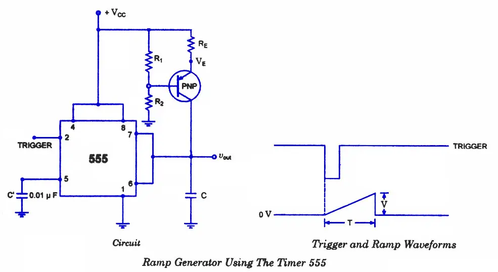
We know that if a capacitor is charged from a voltage source through a resistor, an exponential waveform is produced while charging of a capaci­tor from a constant current source produces a ramp. This is the idea behind the circuit. The circuit of a ramp generator using timer 555 is shown in figure. Here the resistor of previ­ous circuits is replaced by a PNP transistor that produces a constant charging current.

Ramp Generator Circuit

Ramp Generator Circuit

Charging current produced by PNP constant current source is

iC = Vcc-VE / RE

where VE = R2 / (R1 + R2) * VCC + VBE

When a trigger starts the monostable multivibrator timer 555 as shown in figure, the PNP current source forces a constant charging into the capacitor C. The voltage across the capacitor is, therefore, a ramp as illustrated in the figure. The slope of the ramp is given as

Slope, s = I/C