Showing posts with label electronic circuits. Show all posts
Sunday, October 11, 2009

Circuit Diagram of a LED sequencer

LED sequencer

PARTS AND MATERIALS

  • 4017 decade counter/divider (Radio Shack catalog # 276-2417)
  • 555 timer IC (Radio Shack catalog # 276-1723)
  • Ten-segment bargraph LED (Radio Shack catalog # 276-081)
  • One SPST switch
  • One 6 volt battery
  • 10 kΩ resistor
  • 1 MΩ resistor
  • 0.1 µF capacitor (Radio Shack catalog # 272-135 or equivalent)
  • Coupling capacitor, 0.047 to 0.001 µF
  • Ten 470 Ω resistors
  • Audio detector with headphones

Caution! The 4017 IC is CMOS, and therefore sensitive to static electricity!

Any single-pole, single-throw switch is adequate. A household light switch will work fine, and is readily available at any hardware store.

The audio detector will be used to assess signal frequency. If you have access to an oscilloscope, the audio detector is unnecessary.


CROSS-REFERENCES

Lessons In Electric Circuits, Volume 4, chapter 3: "Logic Gates"

Lessons In Electric Circuits, Volume 4, chapter 4: "Switches"

Lessons In Electric Circuits, Volume 4, chapter 11: "Counters"


LEARNING OBJECTIVES

  • Use of a 555 timer circuit to produce "clock" pulses (astable multivibrator)
  • Use of a 4017 decade counter/divider circuit to produce a sequence of pulses
  • Use of a 4017 decade counter/divider circuit for frequency division
  • Using a frequency divider and timepiece (watch) to measure frequency
  • Purpose of a "pulldown" resistor
  • Learn the effects of switch contact "bounce" on digital circuits
  • Use of a 555 timer circuit to "debounce" a mechanical switch (monostable multivibrator)

SCHEMATIC DIAGRAM


ILLUSTRATION


INSTRUCTIONS

The model 4017 integrated circuit is a CMOS counter with ten output terminals. One of these ten terminals will be in a "high" state at any given time, with all others being "low," giving a "one-of-ten" output sequence. If low-to-high voltage pulses are applied to the "clock" (Clk) terminal of the 4017, it will increment its count, forcing the next output into a "high" state.

With a 555 timer connected as an astable multivibrator (oscillator) of low frequency, the 4017 will cycle through its ten-count sequence, lighting up each LED, one at a time, and "recycling" back to the first LED. The result is a visually pleasing sequence of flashing lights. Feel free to experiment with resistor and capacitor values on the 555 timer to create different flash rates.

Try disconnecting the jumper wire leading from the 4017's "Clock" terminal (pin #14) to the 555's "Output" terminal (pin #3) where it connects to the 555 timer chip, and hold its end in your hand. If there is sufficient 60 Hz power-line "noise" around you, the 4017 will detect it as a fast clock signal, causing the LEDs to blink very rapidly.

Two terminals on the 4017 chip, "Reset" and "Clock Enable," are maintained in a "low" state by means of a connection to the negative side of the battery (ground). This is necessary if the chip is to count freely. If the "Reset" terminal is made "high," the 4017's output will be reset back to 0 (pin #3 "high," all other output pins "low"). If the "Clock Enable" is made "high," the chip will stop responding to the clock signal and pause in its counting sequence.

If the 4017's "Reset" terminal is connected to one of its ten output terminals, its counting sequence will be cut short, or truncated. You may experiment with this by disconnecting the "Reset" terminal from ground, then connecting a long jumper wire to the "Reset" terminal for easy connection to the outputs at the ten-segment LED bargraph. Notice how many (or how few) LEDs light up with the "Reset" connected to any one of the outputs:

Counters such as the 4017 may be used as digital frequency dividers, to take a clock signal and produce a pulse occurring at some integer factor of the clock frequency. For example, if the clock signal from the 555 timer is 200 Hz, and the 4017 is configured for a full-count sequence (the "Reset" terminal connected to ground, giving a full, ten-step count), a signal with a period ten times as long (20 Hz) will be present at any of the 4017's output terminals. In other words, each output terminal will cycle once for every ten cycles of the clock signal: a frequency ten times as slow.

To experiment with this principle, connect your audio detector between output 0 (pin #3) of the 4017 and ground, through a very small capacitor (0.047 µF to 0.001 µF). The capacitor is used for "coupling" AC signals only, to that you may audibly detect pulses without placing a DC (resistive) load on the counter chip output. With the 4017 "Reset" terminal grounded, you will have a full-count sequence, and you will hear a "click" in the headphones every time the "0" LED lights up, corresponding to 1/10 of the 555's actual output frequency:

In fact, knowing this mathematical relationship between clicks heard in the headphone and the clock frequency allows us to measure the clock frequency to a fair degree of precision. Using a stopwatch or other timepiece, count the number of clicks heard in one full minute while connected to the 4017's "0" output. Using a 1 MΩ resistor and 0.1 µF capacitor in the 555 timing circuit, and a power supply voltage of 13 volts (instead of 6), I counted 79 clicks in one minute from my circuit. Your circuit may produce slightly different results. Multiply the number of pulses counted at the "0" output by 10 to obtain the number of cycles produced by the 555 timer during that same time (my circuit: 79 x 10 = 790 cycles). Divide this number by 60 to obtain the number of timer cycles elapsed in each second (my circuit: 790/60 = 13.17). This final figure is the clock frequency in Hz.

Now, leaving one test probe of the audio detector connected to ground, take the other test probe (the one with the coupling capacitor connected in series) and connect it to pin #3 of the 555 timer. The buzzing you hear is the undivided clock frequency:

By connecting the 4017's "Reset" terminal to one of the output terminals, a truncated sequence will result. If we are using the 4017 as a frequency divider, this means the output frequency will be a different factor of the clock frequency: 1/9, 1/8, 1/7, 1/6, 1/5, 1/4, 1/3, or 1/2, depending on which output terminal we connect the "Reset" jumper wire to. Re-connect the audio detector test probe to output "0" of the 4017 (pin #3), and connect the "Reset" terminal jumper to the sixth LED from the left on the bargraph. This should produce a 1/5 frequency division ratio:

Counting the number of clicks heard in one minute again, you should obtain a number approximately twice as large as what was counted with the 4017 configured for a 1/10 ratio, because 1/5 is twice as large a ratio as 1/10. If you do not obtain a count that is exactly twice what you obtained before, it is because of error inherent to the method of counting cycles: coordinating your sense of hearing with the display of a stopwatch or other time-keeping device.

Try replacing the 1 MΩ timing resistor in the 555 circuit with one of greatly lesser value, such as 10 kΩ. This will increase the clock frequency driving the 4017 chip. Use the audio detector to listen to the divided frequency at pin #3 of the 4017, noting the different tones produced as you move the "Reset" jumper wire to different outputs, creating different frequency division ratios. See if you can produce octaves by dividing the original frequency by 2, then by 4, and then by 8 (each descending octave represents one-half the previous frequency). Octaves are readily distinguished from other divided frequencies by their similar pitches to the original tone.

A final lesson that may be learned from this circuit is that of switch contact "bounce." For this, you will need a switch to provide clock signals to the 4017 chip, instead of the 555 timer. Re-connect the "Reset" jumper wire to ground to enable a full ten-step count sequence, and disconnect the 555's output from the 4017's "Clock" input terminal. Connect a switch in series with a 10 kΩ pulldown resistor, and connect this assembly to the 4017 "Clock" input as shown:

The purpose of a "pulldown" resistor is to provide a definite "low" logic state when the switch contact opens. Without this resistor in place, the 4017's "Clock" input wire would be floating whenever the switch contact was opened, leaving it susceptible to interference from stray static voltages or electrical "noise," either one capable of making the 4017 count randomly. With the pulldown resistor in place, the 4017's "Clock" input will have a definite, albeit resistive, connection to ground, providing a stable "low" logic state that precludes any interference from static electricity or "noise" coupled from nearby AC circuit wiring.

Actuate the switch on and off, noting the action of the LEDs. With each off-to-on switch transition, the 4017 should increment once in its count. However, you may notice some strange behavior: sometimes, the LED sequence will "skip" one or even several steps with a single switch closure. Why is this? It is due to very rapid, mechanical "bouncing" of the switch contacts. When two metallic contacts are brought together rapidly as does happen inside most switches, there will be an elastic collision. This collision results in the contacts making and breaking very rapidly as they "bounce" off one another. Normally, this "bouncing" is much to rapid for you to see its effects, but in a digital circuit such as this where the counter chip is able to respond to very quick clock pulses, these "bounces" are interpreted as distinct clock signals, and the count incremented accordingly.

One way to combat this problem is to use a timing circuit to produce a single pulse for any number of input pulse signals received within a short amount of time. The circuit is called a monostable multivibrator, and any technique eliminating the false pulses caused by switch contact "bounce" is called debouncing.

The 555 timer circuit is capable of functioning as a debouncer, if the "Trigger" input is connected to the switch as such:

Please note that since we are using the 555 once again to provide a clock signal to the 4017, we must re-connect pin #3 of the 555 chip to pin #14 of the 4017 chip! Also, if you have altered the values of the resistor or capacitor in the 555 timer circuit, you should return to the original 1 MΩ and 0.1 µF components.

Actuate the switch again and note the counting behavior of the 4017. There should be no more "skipped" counts as there were before, because the 555 timer outputs a single, crisp pulse for every on-to-offactuation (notice the inversion of operation here!) of the switch. It is important that the timing of the 555 circuit be appropriate: the time to charge the capacitor should be longer than the "settling" period of the switch (the time required for the contacts to stop bouncing), but not so long that the timer would "miss" a rapid sequence of switch actuations, if they were to occur.

7-segment display

PARTS AND MATERIALS

  • 4511 BCD-to-7seg latch/decoder/driver (Radio Shack catalog # 900-4437)
  • Common-cathode 7-segment LED display (Radio Shack catalog # 276-075)
  • Eight-position DIP switch (Radio Shack catalog # 275-1301)
  • Four 10 kΩ resistors
  • Seven 470 Ω resistors
  • One 6 volt battery

Caution! The 4511 IC is CMOS, and therefore sensitive to static electricity!


CROSS-REFERENCES

Lessons In Electric Circuits, Volume 4, chapter 9: "Combinational Logic Functions"


LEARNING OBJECTIVES

  • How to use the 4511 7-segment decoder/display driver IC
  • Gain familiarity with the BCD code
  • How to use 7-segment LED assemblies to create decimal digit displays
  • How to identify and use both "active-low" and "active-high" logic inputs

SCHEMATIC DIAGRAM


ILLUSTRATION


INSTRUCTIONS

This experiment is more of an introduction to the 4511 decoder/display driver IC than it is a lesson in how to "build up" a digital function from lower-level components. Since 7-segment displays are very common components of digital devices, it is good to be familiar with the "driving" circuits behind them, and the 4511 is a good example of a typical driver IC.

Its operating principle is to input a four-bit BCD (Binary-Coded Decimal) value, and energize the proper output lines to form the corresponding decimal digit on the 7-segment LED display. The BCD inputs are designated A, B, C, and D in order from least-significant to most-significant. Outputs are labeled a, b, c, d, e, f, and g, each letter corresponding to a standardized segment designation for 7-segment displays. Of course, since each LED segment requires its own dropping resistor, we must use seven 470 Ω resistors placed in series between the 4511's output terminals and the corresponding terminals of the display unit.

Most 7-segment displays also provide for a decimal point (sometimes two!), a separate LED and terminal designated for its operation. All LEDs inside the display unit are made common to each other on one side, either cathode or anode. The 4511 display driver IC requires a common-cathode 7-segment display unit, and so that is what is used here.

After building the circuit and applying power, operate the four switches in a binary counting sequence (0000 to 1111), noting the 7-segment display. A 0000 input should result in a decimal "0" display, a 0001 input should result in a decimal "1" display, and so on through 1001 (decimal "9"). What happens for the binary numbers 1010 (10) through 1111 (15)? Read the datasheet on the 4511 IC and see what the manufacturer specifies for operation above an input value of 9. In the BCD code, there is no real meaning for 1010, 1011, 1100, 1101, 1110, or 1111. These are binary values beyond the range of a single decimal digit, and so have no function in a BCD system. The 4511 IC is built to recognize this, and output (or not output!) accordingly.

Three inputs on the 4511 chip have been permanently connected to either Vdd or ground: the "Lamp Test," "Blanking Input," and "Latch Enable." To learn what these inputs do, remove the short jumpers connecting them to either power supply rail (one at a time!), and replace the short jumper with a longer one that can reach the other power supply rail. For example, remove the short jumper connecting the "Latch Enable" input (pin #5) to ground, and replace it with a long jumper wire that can reach all the way to the Vdd power supply rail. Experiment with making this input "high" and "low," observing the results on the 7-segment display as you alter the BCD code with the four input switches. After you've learned what the input's function is, connect it to the power supply rail enabling normal operation, and proceed to experiment with the next input (either "Lamp Test" or "Blanking Input").

Once again, the manufacturer's datasheet will be informative as to the purpose of each of these three inputs. Note that the "Lamp Test" (LT) and "Blanking Input" (BI) input labels are written with boolean complementation bars over the abbreviations. Bar symbols designate these inputs as active-low, meaning that you must make each one "low" in order to invoke its particular function. Making an active-low input "high" places that particular input into a "passive" state where its function will not be invoked. Conversely, the "Latch Enable" (LE) input has no complementation bar written over its abbreviation, and correspondingly it is shown connected to ground ("low") in the schematic so as to not invoke that function. The "Latch Enable" input is an active-high input, which means it must be made "high" (connected to Vdd) in order to invoke its function.

Musical keyboard as a signal generator

PARTS AND MATERIALS

  • Electronic "keyboard" (musical)
  • "Mono" (not stereo) headphone-type plug
  • Impedance matching transformer (1k Ω to 8 Ω ratio; Radio Shack catalog # 273-1380)
  • 10 kΩ resistor

In this experiment, you'll learn how to use an electronic musical keyboard as a source of variable-frequency AC voltage signals. You need not purchase an expensive keyboard for this -- but one with at least a few dozen "voice" selections (piano, flute, harp, etc.) would be good. The "mono" plug will be plugged into the headphone jack of the musical keyboard, so get a plug that's the correct size for the keyboard.

The "impedance matching transformer" is a small-size transformer easily obtained from an electronics supply store. One may be scavenged from a small, junk radio: it connects between the speaker and the circuit board (amplifier), so is easily identifiable by location. The primary winding is rated in ohms of impedance (1000 Ω), and is usually center-tapped. The secondary winding is 8 Ω and not center-tapped. These impedance figures are not the same as DC resistance, so don't expect to read 1000 Ω and 8 Ω with your ohmmeter -- however, the 1000 Ω winding will read more resistance than the 8 Ω winding, because it has more turns.

If such a transformer cannot be obtained for the experiment, a regular 120V/6V step-down power transformer works fairly well, too.


CROSS-REFERENCES

Lessons In Electric Circuits, Volume 2, chapter 1: "Basic AC Theory"

Lessons In Electric Circuits, Volume 2, chapter 7: "Mixed-Frequency AC Signals"


LEARNING OBJECTIVES

  • Difference between amplitude and frequency
  • Measuring AC voltage, current with a meter
  • Transformer operation, step-up

SCHEMATIC DIAGRAM


ILLUSTRATION


INSTRUCTIONS

Normally, a student of electronics in a school would have access to a device called a signal generator, orfunction generator, used to make variable-frequency voltage waveforms to power AC circuits. An inexpensive electronic keyboard is a cheaper alternative to a regular signal generator, and provides features that most signal generators cannot match, such as producing mixed-frequency waves.

To "tap in" to the AC voltage produced by the keyboard, you'll need to insert a plug into the headphone jack (sometimes just labeled "phone" on the keyboard) complete with two wires for connection to circuits of your own design. When you insert the plug into the jack, the normal speaker built in to the keyboard will be disconnected (assuming the keyboard is equipped with one), and the signal that used to power that speaker will be available at the plug wires. In this particular experiment, I recommend using the keyboard to power the 8 Ω side of an audio "output" transformer to step up voltage to a higher level. If using a power transformer instead of an audio output transformer, connect the keyboard to the low-voltage winding so that it operates as a step-up device. Keyboards produce very low voltage signals, so there is no shock hazard in this experiment.

Using an inexpensive Yamaha keyboard, I have found that the "panflute" voice setting produces the truest sine-wave waveform. This waveform, or something close to it (flute, for example), is recommended to start experimenting with since it is relatively free of harmonics (many waveforms mixed together, of integer-multiple frequency). Being composed of just one frequency, it is a less complex waveform for your multimeter to measure. Make sure the keyboard is set to a mode where the note will be sustained as any key is held down -- otherwise, the amplitude (voltage) of the waveform will be constantly changing (high when the key is first pressed, then decaying rapidly to zero).

Using an AC voltmeter, read the voltage direct from the headphone plug. Then, read the voltage as stepped up by the transformer, noting the step ratio. If your multimeter has a "frequency" function, use it to measure the frequency of the waveform produced by the keyboard. Try different notes on the keyboard and record their frequencies. Do you notice a pattern in frequency as you activate different notes, especially keys that are similar to each other (notice the 12-key black-and-white pattern repeated on the keyboard from left to right)? If you don't mind making marks on your keyboard, write the frequencies in Hertz in black ink on the white keys, near the tops where fingers are less likely to rub the numbers off.

Ideally, there should be no change in signal amplitude (voltage) as different frequencies (notes on the keyboard) are tried. If you adjust the volume up and down, you should discover that changes in amplitude should have little or no impact on frequency measurement. Amplitude and frequency are two completely independent aspects of an AC signal.

Try connecting the keyboard output to a 10 kΩ load resistance (through the headphone plug), and measure AC current with your multimeter. If your multimeter has a frequency function, you can measure the frequency of this current as well. It should be the same as for the voltage for any given note (keyboard key).

Design:
Voltage Peak detector

1. Vcc = 12v.

2. Choose VCQ1 output, = 9v.

3. Choose VBQ1 = 8v.

4. VEQ1 = 7.3v.

5. choose RCQ1 = 470 ohms. (to drive a LED output)

6. IRCQ1 = (Vcc - VCQ1) / RCQ1 = ~ 6.38 mA.

7. RE is a split resistance, between the emitter of Q1 and Q2.
RE = ( REQ1 + REQ2) = (VEQ1 / IRCQ1) = ~ 1143 ohms.
So make REQ1 = REQ2 = 560 ohms each.

8. Now VEQ2 = ~ 3.65v.

9. Now with around 1100 ohms for RE, then make RB1Q1 around 2 times RE =~ 2K ohms.

10 IRB1Q1 = (VBQ1 / RB1Q1) = 4mA.

11. RB2Q1 = (Vcc - VBQ1) / IRB1Q1 = 1K ohms.

By varying the resistor value of REQ2, to a higher value, will increase VEQ2, which in turn will then detect a higher PK input voltage.

This will also raise the idle (standing voltage) at the output too.


Idle output voltage.
Input @ 4v.
No trigger of circuit.

Click image for larger version  Name: idle volt.jpg Views: 28 Size: 73.9 KB ID: 192


Input voltagte @ 4.3V.
The circuit is triggered.

Click image for larger version  Name: PK volt.jpg Views: 23 Size: 73.9 KB ID: 193
Tuesday, September 29, 2009

BATTERY CHARGER REGULATOR

This circuit comes from some years ago as a part of a project we did to make it possible to keep a charger on a battery continuously without it overcharging.

It's mostly a junk box project, at least as far as the components used in the one I held onto. This is like late 1970's technology grafted onto 1960's.

The regulator board is a replacement for whatever was in an old Monkey Ward (that is properly Mongomery Ward) charger, rated at 15 amps. The components labelled T1, D1 & 2, Q3, SW1, the ammeter, and the circuit breaker are all part of the charger.

Other components:

Resistors R1 - 7 - 5% carbon 1/2 watt (1/4 watt should be fine)
Resistors R8 & 10 - 1% 1/4 watt. Oops, R10 should be 2.26K
Trimmer R9 - any multi-turn trimmer will do. Single-turn is not good.
Op amp Z1 - any Op amp should do, as long as it's better than a 741. It's used as a comparator, so good input impedance is better. The CA3140 was the hot op amp back when.
D3 - any 2.5 volt reference diode will do.
D4 - any 1N400X will do.
D5 - this is a 4.7 volt zener. $00 mw is fine - no tolerance necessary.
Q1 - we had cases of 2N1613's. Used them for everything. It's a switch, so 2N2222 is a good sub.
Q2 - had bunches of these, too. Just about any PNP will sub.

Operation:

The output from the full wave rectifiers is pulsating DC. The diode D4 isolates the op amp from these pulsations, and C1 filters it. Z1 is set up as a comparator with the D3 reference diode presenting 2.5 volts to pin 3. As long as the voltage on pin 2 is less than that, the output will be high.

In operation (with the switch in the regulated position) the voltage on pin 2 will reflect the charge on the battery during the low portion of the rectified waveform. If it is less than 2.5 volts, as set by the R9 trimmer, then Z1 output wil be high. That will turn on Q1. In turn, that will turn on Q2. As the rectified voltage increases, so will the voltage between R6 & 7. This will gate Q3 and allow charge to flow to the battery.

When the battery is up to charge (ideally, 13.6 volts), the voltage on pin 2 of Z2 will be high enough to make the output go low. This will leave Q1 & 2 off, and the SCR will not gate again until the battery charge falls a bit lower.

By using a meter, R9 may be adjusted for a very precise charge on the battery.
My first project with an ATMEL AVR microcontroller (ATMega8). I use the DS1820 digital temperature meter.
Monday, September 28, 2009

Simple Ding-Dong Bell

Simple Ding-Dong Bell

Description

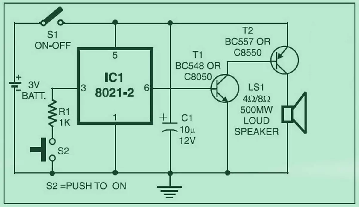
Here we present a simple an low cost ding dong bell suitable for calling bell purposes.It is made around IC 8021-2 .It is a 8 pin IC but only four pins are shown here. 8021 has an in-built circuitry to produce ding dong sound each time its pin 3 is pulled low.The sound is stored in a 4 bit ROM.a complementary-pair, two-transistor amplifier is used to amplify the sound to a fair level of audibility.A piezo
tweeter or an 8-ohm, 500mW speaker can be used at the output.

Each time when switch S2 is pressed, ding dong sound is produced twice. If you try to press switch S2 a second time when the first ding dong sound is still being produed, it has no effect whatever and the two ding-dong bell sounds will be invariably produced.S1 is the ON- OFF switch.Assemble the circuit on a good quality all pupose PCB.Don’t forget to use an IC holder for IC 8021.

Circuit Diagram. Click to view larger.

ding-dong.jpg

Jet engine sound generator

Description.
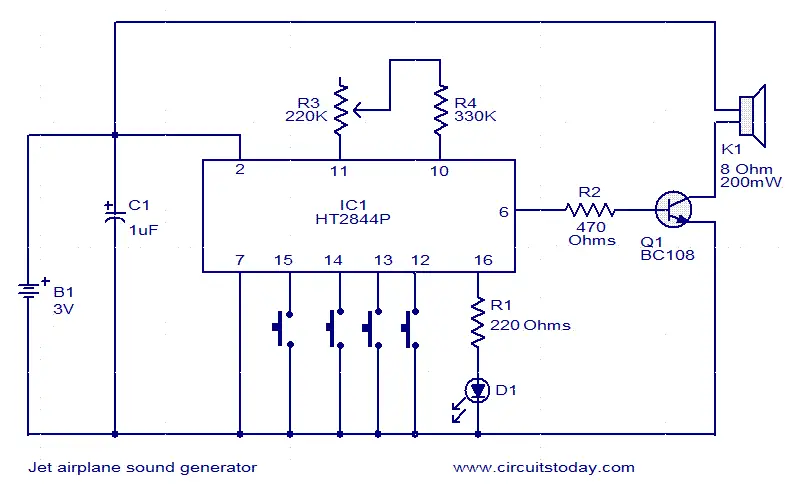
This jet engine sound generator circuit is based on the sound generator IC HT2844P from Holtek Semiconductors. This particular IC can make four sounds namely low speed sound of jet engine, high speed sound of jet engine, missile sound and machine gun sound. Each of these sounds can be activated by connecting the pins 12, 13, 14and 15 to ground by using the respective push button switches. Resistor R3 can be used for manually increasing or decreasing the speed.LED D1 gives a visible indication of the sound.

Circuit diagram.

jet-engine-sound-generator

Notes.

  • The circuit can be powered from a 3V battery.
  • Do not give more than 3.3V to the IC.
  • K1 can be a 200mW/8 Ohm speaker.
  • IC1 must be mounted on a holder.

Water level alarm circuit

Description.

Here is a simple water level alarm circuit that will produce an audible alarm when the water level reaches a preset level.The circuit can be powered of a 3V battery and is very handy to use.

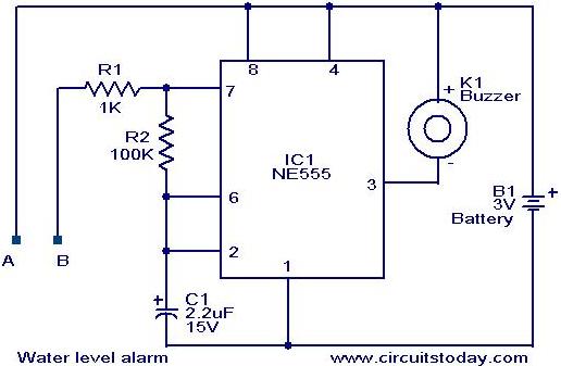
The circuit is based on an astable multivibrator wired around IC1 (NE 555).The operating frequency of the astable multivibrator here will depend on capacitor C1, resistances R1,R2 and the resistance across the probes A&B.When there is no water up to the probes,they will be open and so the multivibrator will not produce oscillations and the buzzer will not beep.When there is water up to the level of probes,some current will pass through the water,the circuit will be closed to some extend,and the IC will start producing oscillations in a frequency proportional to the value of C1,R1,R2 and the resistance of water across the probes.The buzzer will beep to indicate the presence of water up to the level of the sensing probes.

Circuit diagram with Parts list.

water-level-alarm-circuit.JPG

Notes.

  • The circuit can be powered of a 3V battery.
  • Assemble the circuit on a good quality PCB or common board.
  • The probes can be made of two insulated copper Aluminiun wires.
  • Place the probes at the position where you have to sense the level.

Simple Electronic Combination Lock using IC LS 7220

Description

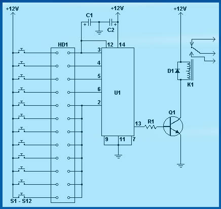
This is the circuit diagram of a simple electronic combination lock using IC LS 7220.This circuit can be used to activate a relay for controlling (on & off) any device when a preset combination of 4 digits are pressed.The circuit can be operated from 5V to 12V.

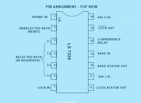
To set the combination connect the appropriate switches to pin 3,4,5 and 6 of the IC through the header.As an example if S1 is connected to pin 3, S2 to pin 4 , S3 to pin 5, S4 to pin 6 of the IC ,the combination will be 1234.This way we can create any 4 digit combinations.Then connect the rest of the switches to pin 2 of IC.This will cause the IC to reset if any invalid key is pressed , and entire key code has to be re entered.

When the correct key combination is pressed the out put ( relay) will be activated for a preset time determined by the capacitor C1.Here it is set to be 6S.Increase C1 to increase on time.

For the key pad, arrange switches in a 3X4 matrix on a PCB.Write the digits on the keys using a marker.Instead of using numbers I wrote some symbols!.The bad guys will be more confused by this.

Circuit Diagram . Click image to Enlarge. Pin Assignment of LS7220.

lock-ls-7220.jpg ls-7220-pin-ass.jpg
Parts List

C1 1 1uF 25V Electrolytic Capacitor
C2 1 220uF 25V Electrolytic Capacitor
R1 1 2.2K 1/4W Resistor
Q1 1 2N3904 NPN Transistor 2N2222
D1 1 1N4148 Rectifier Diode 1N4001-1N4007
K1 1 12V SPDT Relay Any appropriate relay with 12V coil
U1 1 LS7220 Digital Lock IC
S1-S12 12 SPST Momentary Pushbutton Keypad (see notes)
HD1 1 12 Position Header

Remote control tester circuit

Description.

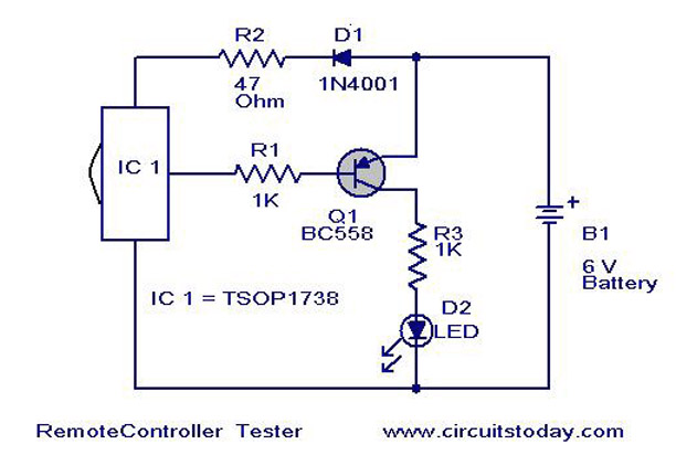
This is a simple remote controller tester circuit based on infrared sensor IC TSOP 1738. When the IR waves fall on the sensor it output changes to low state.This makes the transistor Q1 ON and LED will blink according to the code contained in the signal.So for press of each button the LED blinks in different ways.This is a good indication of the working of remote.The diode D1drops 0.7 V to give the IC ~ 5V supply from the available 6V .R2 is a current limiting resistance.

Circuit Diagram with Parts List .

remote-control-tester-circuit.jpg

Notes .

  • Use a 6V battery to power up the circuit.
  • This circuit can be used to test remotes operating in the 38Khz carrier frequency.Almost all remotes fall into this category so no problem.

Single Chip FM Radio circuit

Description.

Here is a compact low cost FM radio circuit using IC7400. This circuit is designed as per the data sheet and the result is excellent.Ideal for all category of electronic enthusiasts.

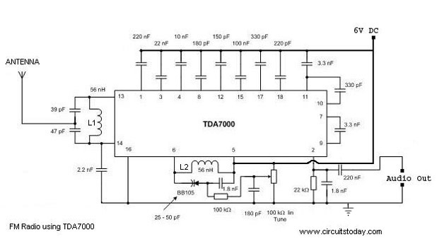
The TDA7000 is a monolithic integrated circuit for mono FM portable radios, where a minimum on peripheral components is crucial. The IC TDA 7000 has a Frequency-Locked-Loop system with an intermediate frequency of 70 kHz. The intermediate frequency selectivity is achieved by active RC filters. The only function which needs alignment is the resonant circuit for the oscillator, thus selecting the reception frequency. Spurious reception is avoided by means of a mute circuit, which also eliminates too noisy input signals. Special steps are taken to meet the radiation requirements.

Circuit Diagram with Parts List. tda-7000-fm-radio-1.jpg

Notes

  • For L1 and L2 wind 5 turns of 0.6 mm enameled Copper wire on a 4 mm dia plastic former.
  • For antenna use a 50mm long insulated copper wire.
  • IC TDA 7000 can withstand up to 10 V supply voltage.But I recommend 6V.
  • Use an 8 Ohm speaker or Headphone at the audio output.

Lead acid battery charger circuit

Description

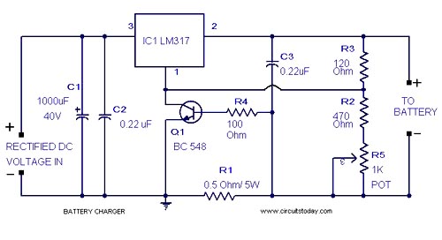
Here is a lead acid battery charger circuit using IC LM 317.The IC here provides the correct charging voltage for the battery.A battery must be charged with 1/10 its Ah value.This charging circuit is designed based on this fact.The charging curent for the battery is controlled by Q1 ,R1,R4 and R5. Potentiometer R5 can be used to set the charging current.As the battery gets charged the the current through R1 increases .This changes the conduction of Q1.Since collector of Q1 is connected to adjust pin of IC LM 317 the voltage at the output of of LM 317 increases.When battery is fully charged charger circuit reduces the charging current and this mode is called trickle charging mode.

Circuit Diagram with Parts List.

battery-charger.jpg

Notes .

  • Connect a battery to the circuit in series with a ammeter.Now adjust R5 to get the required charging current. Charging current = (1/10)*Ah value of battery.
  • Input to the IC must be minimum 15V to get 12 V for charging the battery .Take a look at the data sheet of LM 317 for better understanding.
  • Fix LM317 with a heat sink.

Car battery Volt meter circuit using LED

Description

This is a very useful circuit which when installed on your car gives the voltage of you car battery in a LED dot display form.The circuit is based on four comparators made of quad op amp LM324.The inverting inputs of IC are kept at at reference voltages 5.6V,5.2V,4.8V,4.4V respectively at pins 2,6,9,13 by resistors ,R3,R4,R5,R6.The battery voltage is directly fed to the nin inverting input throug the volatge divider arrangement using R1 and R7.When there is variation in the input supply the out put of each op amp goes high accordingly as they are wired as voltage comparators.The corresponding LED glows.

Circuit Diagram and Parts List

led-volt-meter.jpg

Notes

  • IC LM 324 consists of4 op amps in one package , so power supply is common and is shown once (pin 4 and 11).
  • To setup , connect the circuit to battery ,adjust R6 so that required voltages are available at the inverting pins( refer description to get the required voltages).
  • Fix the LED’s on the dash board and mark the voltages near to it as shown in circuit diagram.The gadget is now ready.

Simple Lamp Dimmer/ Fan Regulator

Description .

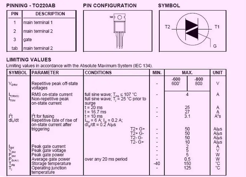
This is the circuit diagram of the simplest lamp dimmer or fan regulator.The circuit is based on the principle of power control using a Triac.The circuit works by varying the firing angle of the Triac . Resistors R1 ,R2 and capacitor C2 are associated with this.The firing angle can be varied by varying the value of any of these components.Here R1 is selected as the variable element .By varying the value of R1 the firing angle of Triac changes (in simple words, how much time should Triac conduct) changes.This directly varies the load power, since load is driven by Triac.The firing pulses are given to the gate of Triac T1 using Diac D1.

Notes

Assemble the circuit on a good quality PCB or common board.The load whether lamp ,fan or any thing ,should be less than 200 Watts.To connect higher loads replace the Triac BT 136 with a higher Watt capacity Triac . All parts of the circuit are active with potential shock hazard.So be careful.

I advice to test the circuit with a low voltage supply (say 12V or 24V AC) and a small load (a same volt bulb) ,before connecting the circuit to mains.

Parts List

R1 1o K 1 Watt Resistor

R2 1o0 K Potentiometer (Variable Resistance)

C1 0.1 uF (500V or above ) Polyester Capacitor

T1 BT 136 Triac

D1 DB2 Diac

Circuit Diagram BT 136Triac Necessary Data.

lamp-dimmer.JPG bt.JPG

CLICK THE IMAGES TO ENLARGE

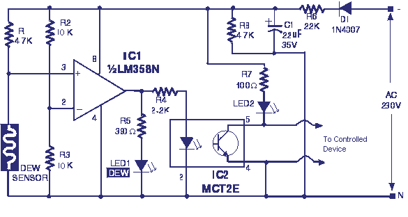
Here is a simple circuit that can be used to switch ON or OFF a device when the dew present in the surrounding atmosphere crosses a set value.The circuit uses a dew sensitive resistive element and a comparator based on LM 358 to perform the above said operation.

At normal condition the resistance of dew sensor element will be low and so the voltage drop across it.So the voltage at the non inverting pin of LM358 (IC1) will be less than the voltage at the inverting input of the LM358.So the output of the opamp will be low.This keeps the opto-coupler (MCT2E) deactivated.When the dew increases the resistance of the element increases and so do the voltage across it.Now the voltage at the non inverting pin of LM358 (IC1) will be higher than the voltage at the inverting input of the LM358.So the output of the op amp will be switched to high.This in turn activates the optocoupler.The LED glows to indicate it. As a result we get an optopcoupler activated and de activated according to the amount of dew in the atmosphere.The output pins of optocoupler pin (5&4) can be used to control the external device.

Diode D1 , resistors R6&R3 and capacitor C1 is employed here to derive the power for the circuit directly from mains.

Circuit diagram with Parts list.

dew-sensor-circuit.gif

Notes.

  • The dew sensor is hard to find in market.But it can be easily obtained from a old VCR.Also the type no of the sensor is not so important here.Try with any thing you get.I used one from a old Hitachi VCR.
  • LM 358 is a dual opamp.Here only one opamp inside it is used.

Story behind this circuit.

One day (when I was in high school) I was doing autopsy on our dead old VCR. Some way I found a component that was not familiar to me.I asked a TV mechanic about this.He said , that was a dew sensor.Suddenly the idea clicked in my mind.Why couldn’t I make a dew sensitive switch using this sensor.The result was great. .Actually in my first prototype there was no opamp or opto-coupler and had only two transistors.One tuned to sense the voltage change across sensor and other to drive a relay.The circuit shown here is a modification later done by me.